
ページ読込中...
ページ読込中...

[English]
| 長谷川 剛 [教授] |  |
|
| homepage | https://thasega.w.waseda.jp/ | |
| 専門分野 | 物性物理学 | |
| 研究テーマ・研究活動 | ||
| 1985年 東京工業大学理学部物理学科卒業 1987年 東京工業大学大学院修士課程修了 1987-1999年 日立製作所中央研究所 1996年 博士(理学)東京工業大学 1999-2002年 理化学研究所 2002-2015年 物質・材料研究機構 2007年 文部科学大臣表彰科学技術賞(研究部門) 2015年 早稲田大学理工学術院 教授 |
||
原子の並び方ひとつで、同じ炭素原子でも、ダイヤモンドにも黒鉛にもなる。私たちが研究しているのは、そんな不思議な世界です。物質の多くは整然と並んだ原子によって構成されていますが、その表面では、物質内部とは異なる原子配列が観察されることがあります。例えば、一見平らな金の表面も原子スケールではノコギリ状であったり、シリコンの表面では原子が大きな格子模様を作っていたりします。百聞は一見に如かず。見ることができれば、沢山のことが明らかになります。新しい構造解析手法を発明した物理学者の多くがノーベル賞に輝いてきた所以です。
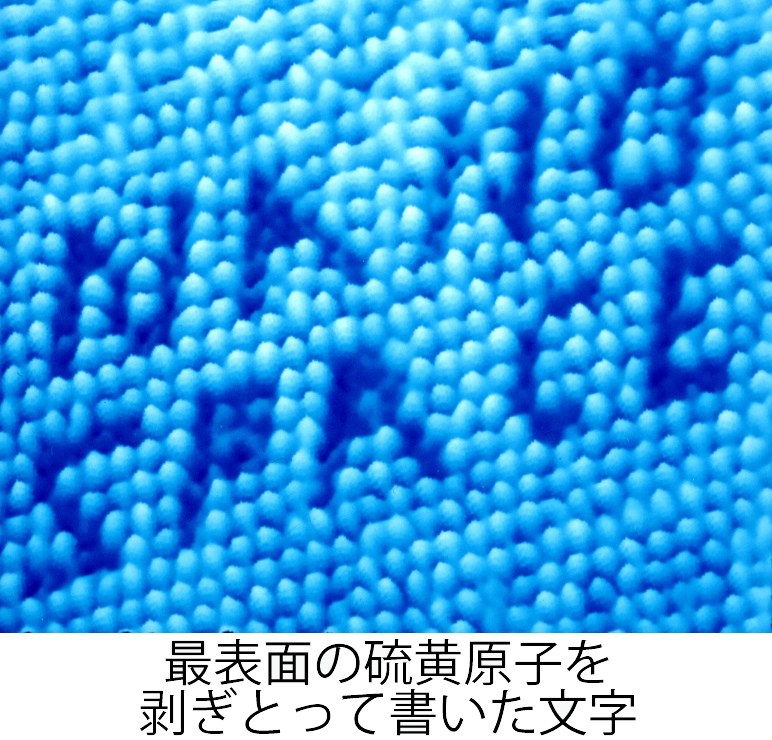
最近では、原子を観るだけでなく、個々の原子を操ることも可能になっています。例えば私たちは、二硫化モリブデンの最表面にある硫黄原子を一つずつ剥ぎ取って「原子文字」を書きました。この実験では、原子レベルで尖った針で表面をなぞって観察する「走査型トンネル顕微鏡」を用いました。原子1個を記憶単位とするメモリの開発が夢です。
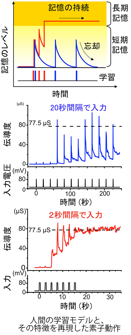
さらに、固体中を行きつ戻りつしながら原子が移動する現象を利用すると、頻繁に電圧を加えるとスイッチオンするが、時間間隔を空けて電圧を加えるといつになってもオンにならない素子も作れます。「電圧」を「学習」に置き換えると、まるで人間が何かを記憶するときと同じ様なことが起きています。
20世紀は、半導体トランジスタを始めとして、「電子」が世界の牽引役でした。一方、21世紀は、燃料電池を始めとして、「原子(イオン)」にも注目が集まっています。原子は、電子の様にトンネル効果によってどこかに行ってしまうことがありません。原子は電子よりもはるかに大きく、重たいですが、それ故に、新しい機能を実現できる可能性があります。私たちは、金属原子の輸送を制御した新しいトランジスタを世界で初めて開発しました。このトランジスタは電源を切ってもオン/オフ状態が保たれるので、起動時間ゼロのパソコンの開発に繋がると期待しています。
見方を変えれば、デメリットもメリットになります。基本物理現象の理解に基づいた新しい概念の創造を私たちと一緒にしませんか?
| Tsuyoshi Hasegawa [Professor] | |
|
| homepage | https://thasega.w.waseda.jp/ | |
| research field | Nano-science, Nano-electronics, Surface physics | |
| research keywords | ||
| Atomic switch Solid-state ionics Scanning probe microscopy Electrochemical reaction |
||
| link | ||
The same carbon atoms can be diamond or graphite depending on how they are arranged in space; the area of research that we pursue is in such a world of wonder. My research began with the graduation research to study the arrangement of atoms on material surfaces with the use of a high-resolution electron microscope. While most materials are composed of atoms in a perfect array, there are cases where atomic arrangements are observed on the surface that are different from those inside the material.
‘Atom manipulation’, which is now considered to be relatively easy to do, was a challenging research subject those days. Fig. 1 shows letters written by removing sulfur atoms from the surface of molybdenum disulfide. I worked on such tasks while I was with the Hitachi Central Research Laboratory. Hitachi values fundamental research, and I am grateful to the company for its extreme generosity.
Now my major research subjects cover clarification of phenomena on the atomic and molecular scale, and applications to devices, including the development of a new nanodevice ‘Atomic Switch’ using the transfer of atoms. I have been continuously engaged in research of ‘Observation of Atoms’, ’Manipulation of Atoms’ and ‘Utilization of Atoms’. Part of the resulting research results are in the process of being utilized for product commercialization for enterprises. All the research results were obtained with the use of uniquely developed equipment, which is required in order to pursue cutting-edge research. The conduct of research refers to reducing the number of black boxes (unknowns) one by one. So far as equipment goes, it is desirable that you should know it well enough to repair yourself, as well as understanding its principles.
We welcome students and young scientists who want to enter the nano-world.