
ページ読込中...
ページ読込中...

[English]
| 竹内 淳 [教授] |  |
|
| homepage | https://atacke.w.waseda.jp/ | |
| 専門分野 | 半導体デバイス研究 | |
| 研究テーマ・研究活動 | ||
| 1985 年 大阪大学大学院基礎工学研究科 博士前期課程修了.富士通研究所入社 1993 年 博士(理学)大阪大学 1993 年 マックスプランク固体研究所(独)客員研究員 電子情報通信学会論文賞 受賞 2002 年 早稲田大学理工学部・教授 2004 年 応用物理学会論文賞JJAP 論文賞 受賞 |
||
みなさんが普段体験する最も短い時間は、どの程度の時間でしょうか。おそらく普通思い浮かべる時間は「一瞬」という時間でしょう。これは、“まばたきするほどの短い間” で、0.1 秒ほどの時間です。それでは、半導体の中で起こるもっとも速い現象はどの程度の時間で起こるのでしょう? 答は、1兆分の1秒程度の時間ということになります。「1兆分の1秒なんて想像もつかない!」というのが多くの人の感想だと思いますが、どうしてそんなに速い現象を調べるのかというと、半導体を使ったさまざまな素子(トランジスタやレーザなど)に、いっそうの高速化が要求されているからです。これらの素子が高速化されれば、より多くの情報をより迅速に処理することが可能になります。伝達される情報量の飛躍的な拡大と高速化は人類の社会に多大な貢献をすることでしょう。
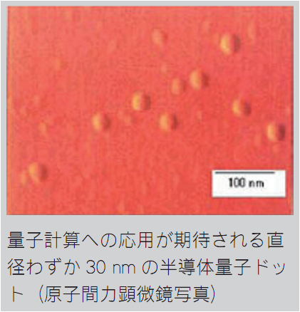
また、半導体はたんに“速い” ということにとどまらず、“非常に小さい” 人工構造物の世界です。次の写真は、量子ドットと呼ばれる微細な構造の写真(原子間力顕微鏡で撮影したもの)で、10 万分の2 ミリほどの大きさに電子の波を閉じ込めます(1nm = 10-9m)。
これを利用して演算を行うと、現在のコンピュータをはるかにしのぐ超高速で大規模な演算が期待できます(量子コンピュータと呼びます)。
半導体の世界ではまた、青色で発光するデバイスの開発が続いています。
Blu-ray DVD などの日本が産んだ新しい技術です。この青色発光半導体の研究にも取り組んでいます。
竹内研究室では、このような微細なナノ構造の中で起こる超高速の現象を調べるために、特殊なレーザから出る光パルスを使っています。光パルスの時間幅は、10 兆分の1秒という極めて短い時間です。超高速の現象を調べ、その物理を探求し、さらに応用に役立てること、それが竹内研究室のテーマです。人類の到達可能な最も速い現象を調べるということは、それだけで充分な知的冒険だと思います。若いみなさんの参加を期待しています。
| Atsushi Tackeuchi [Professor] | |
|
| homepage | https://atacke.w.waseda.jp/ | |
| research field | Manipulation of carriers and spins in semiconductor quantum confined structures | |
| research keywords | ||
| Semiconductor physics Spintronics Ultrafast phenomena |
||
| link | ||
| Research Profiles (at Faculty of Science and Engineering) | ||
Manipulation of electronic spin may provide new flexibility in device operations. Since spin in quantum dots is maintained coherently over nanosecond intervals by three-dimensional quantum confinement effects, the phenomenon may find applications in quantum memory or computing devices. Our research seeks to apply this underdeveloped flexibility for use in future quantum devices and for computing, based on our studies of ultrafast phenomena in semiconductor quantum-confined structures.
At the outset of related work, Tackeuchi realized the inadequacies of conventional time-resolved photoluminescence measurements for observations of very fast picosecond spin relaxation in semiconductors. In response, he proposed and put to use novel pump and probe measurements to observe the spin relaxation of III-V compound semiconductors. He successfully observed for the first time the picosecond spin relaxation process in GaAs quantum wells, InGaAs quantum wells, and bulk GaN. He also demonstrated many interesting aspects of luminescence and tunneling in quantum wells, quantum dots, and the GaN system.
1) “Direct Observation of Picosecond Spin Relaxation of Excitons in GaAs/AlGaAs Quantum Wells using Spin Dependent Optical Nonlinearity,” A. Tackeuchi, S. Muto, T. Inata and T. Fujii, Appl. Phys. Letters 56 (1990) pp. 2213-2215.
” First observations of picosecond spin relaxation in GaAs/AlGaAs quantum wells”
We proposed and demonstrated a novel observation method using a pump and probe technique, which enabled clear observations of picosecond spin relaxation.
2) “Dynamics of Carrier Tunneling between Vertically Aligned Double Quantum Dots,” A. Tackeuchi, T. Kuroda, K. Mase, Y. Nakata, and N. Yokoyama, Phys. Rev. B, 62 (2000) pp. 1568-1571.
“First time-resolved measurement about carrier tunneling between quantum dots”
We demonstrated that tunneling between quantum dots is one order of magnitude slower than between quantum wells.
3) “Electron Spin Relaxation in InGaAs/InP Multiple-quantum Wells,” A. Tackeuchi, O. Wada and Y. Nishikawa, Appl. Phys. Lett. 70 (1997) pp.1131-1133.
“First observation of spin relaxation in InGaAs quantum wells in which the energy bandgap corresponds to the optical communication wavelength of 1.55 micrometers”
4) “Electron Spin Flip by Antiferromagnetic Coupling between Semiconductor Quantum Dots,” A. Tackeuchi, T. Kuroda, Y. Nakata, M. Murayama, T. Kitamura and N. Yokoyama, Jpn. J. Appl. Phys., 42, Part 1, 7A (2003) pp. 4278-4281.
“First observation of formation of antiferromagnetic coupling between semiconductor quantum dots”
Antiferromagnetic coupling between quantum dots is expected to move technology further toward quantum computing.
5) “Subpicosecond exciton spin relaxation in GaN,”T. Kuroda, T. Yabushita, T. Kosuge, A. Tackeuchi, K. Taniguchi, T. Chinone, and N. Horio,Appl. Phys. Lett. 85 (2004) pp.3116-3118.
“First observation of sub-picosecond spin relaxation in semiconductors”
The wurtzite GaN was found to exhibit sub-picosecond spin relaxation.
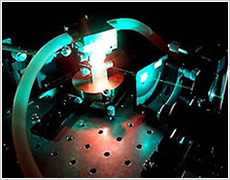
Ti:Sapphire laser (right); quantum dots (up)