
ページ読込中...
ページ読込中...

[English]
| 竹延大志 [教授] |  |
|
| homepage | http://www.f.waseda.jp/takenobu/index.html | |
| 専門分野 | パイ電子材料研究 | |
| 研究テーマ・研究活動 | ||
| 1998 年 北陸先端科学技術大学院大学 材料科学研究科 2001 年 博士課程 博士(材料科学) 2001 年 ソニー株式会社 2001 年 東北大学 金属材料研究所 助手 2007 年 東北大学 金属材料研究所 准教授 2010 年 早稲田大学 理工学術院 先進理工学部 応用物理学科 准教授 2013 年 早稲田大学 理工学術院 先進理工学部 応用物理学科 教授 |
||
有機材料やカーボンナノチューブ等を総じて『パイ電子材料』と呼びます。あまり聞き慣れないかもしれませんが、これらの材料は主に炭素で構成されており、炭素間の結合に『パイ結合』と呼ばれる特徴的な結合を有しているのが理由です。この『パイ電子材料』の特徴を一言で表すと『柔らか
い材料』と言えます。これは、無機材料に比べて様々な現象がより小さなエネルギー領域で支配されている事に由来しています。例えば、これらの材料は互いの相互作用が弱く、様々な有機溶剤に可溶です。また、弱い相互作用は、プラスチックに代表されるような機械的な柔軟性にもつながります。近年では、このような『パイ電子材料』に特徴的な『可溶性』や『柔軟性』を活かした、全く新しい大胆なエレクトロニクスが提唱されています。『可溶性』を活かして、インクのように『パイ電子材料』の溶液を利用し、インクジェット法に代表される印刷技術を用いて電子素子を作製する『プリンタブルエレクトロニクス』が注目されています。必要量の材料を、必要な場所にだけ滴下するインクジェット法は、材料に無駄が出ないため、画期的な省資源・省エネルギーな方法として実現が期待されています。また、紙のように柔らかいプラスチック基板上に電子素子を作製する、『柔軟性』を活かした『フレキシブルエレクトロニクス』(曲げられるエレクトロニクス)という概念も提案されています。最近では、実際にプラスチック基板上に曲がる有機EL ディスプレイの試作も行われています。普段はコンパクトな筒状に丸めて持ち歩き、必要なときに開いて使用する、そんな時代が来るかもしれません。
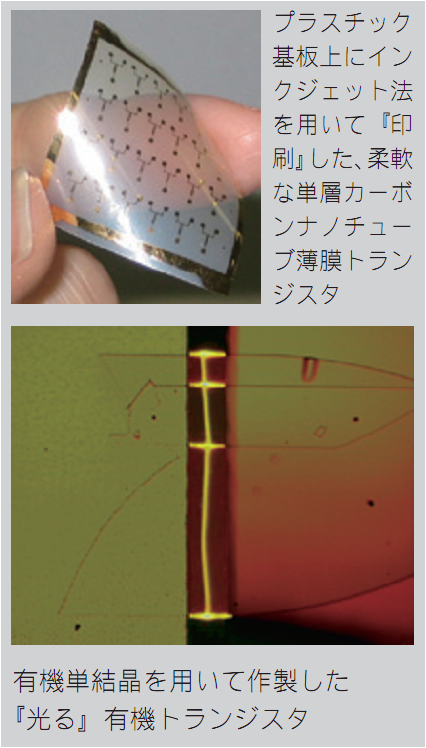
当研究室では、基礎的な物性研究により『パイ電子材料』の本質を理解し、応用研究を通してユニークな特徴を活かした全く新しいエレクトロニクスやオプトエレクトロニクスの提案を目指しています。例えば、単層カーボンナノチューブをインクジェット法でプラスチック基板上に『印刷』し、柔軟なトランジスタの作製に成功しています(図1)。また、有機材料の優れた光機能と電子機能を組み合わせた、光るトランジスタの作製にも成功しています(図2)。どちらも、世界に先駆けた新しい試みです。新しい分野を切り拓くことは、常に未知の困難との闘いです。しかしながら、困難を乗り越えた大きな成功には、それ以上に大きな感動も溢れています。世界を相手にして戦う、気概とやる気に溢れた皆さんの参戦を心待ちしてお
ります。
| Taishi Takenobu [Professor] | |
|
| homepage | http://www.f.waseda.jp/takenobu/index.html | |
| research field | π-electron materials for novel science | |
| research keywords | ||
| π-electron materials Nano-carbon materials Organic devices Flexible electronics Printed electronics |
||
| link | ||
The research in our lab is centered on π-electron materials, such as organic molecules and nano-carbon materials. Our aim is to control and induce novel electronic and photonic responses in these materials. This work combines fundamental studies with forward-looking engineering efforts in a way that promotes positive feedback between the two. Our current research focuses on π-electron materials for novel materials, solid state physics, organic devices, flexible/printed electronics, and electrically driven organic lasers. I would like to explain our five activities very briefly.1. Novel functional Materials
Novel materials can create new physics and new electronics. Sometimes they also change our daily life in drastic ways. We are trying for a synthesis of novel functional materials based on π-electron materials to open up new worlds. You can find one of our reports in Nature Materials 2, 683 – 688 (2003).
2. Physical properties of nano-carbon materials
Nano-carbon materials such as graphene, carbon-nanotubes, and fullerene are very interesting materials that have a different form compared to conventional carbon materials. We are investigating the physical properties (electrical, optical, and magnetic properties) of these materials for future carbon electronics. You can find one of our reports in Physical Review Letters 104, 016803 (2010).
3. Organic devices
Organic materials have unique properties (flexibility and/or printability) compared to conventional inorganic materials such as silicon. Based on the investigated physical properties of organic materials, we are trying to design and fabricate unique organic devices. You can find one of our reports in Nature Materials 3, 317 – 322 (2004).
4. Flexible Electronics/Printed Electronics
Organic materials have flexibility and printability. Such unique properties might create conceptually novel electronics. We are trying to fabricate flexible and/or printed devices using π-electron materials. For example, we are fabricating single-walled carbon-nanotube transistors by inkjet-printing techniques on flexible plastic substrates (see figure). You can find one of our reports in Advanced Materials 22, 3981 3986, (2010).
5. Electrically driven organic laser
One of the biggest advantages of organic materials is their excellent luminescent properties, which are well known for organic light-emitting diodes. However, an electrical driven organic laser has not yet been realized. Although there are many reasons why light-emitting diodes cannot achieve organic laser devices, most of these problems are easily solved in transistor structures. Therefore, we are trying to first create an electrical driven organic laser using organic single-crystal ambipolar transistors. You can find one of our reports in Physical Reveview Letters 100, 066601 (2008).
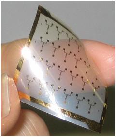
Inkjet-printed carbon-nanotube transistors on the flexible plastic substrate.