北 智洋 教授
Tomohiro Kita
専門分野
光集積デバイス
小さなチップで光を操り、次の社会をつくる技術へ
研究テーマ
通信及びセンシングを目的とした光集積回路の研究
キーワード
光集積回路, シリコンフォトニクス, 非線形光学効果
LINKS
RESEARCH OVERVIEW
研究概要
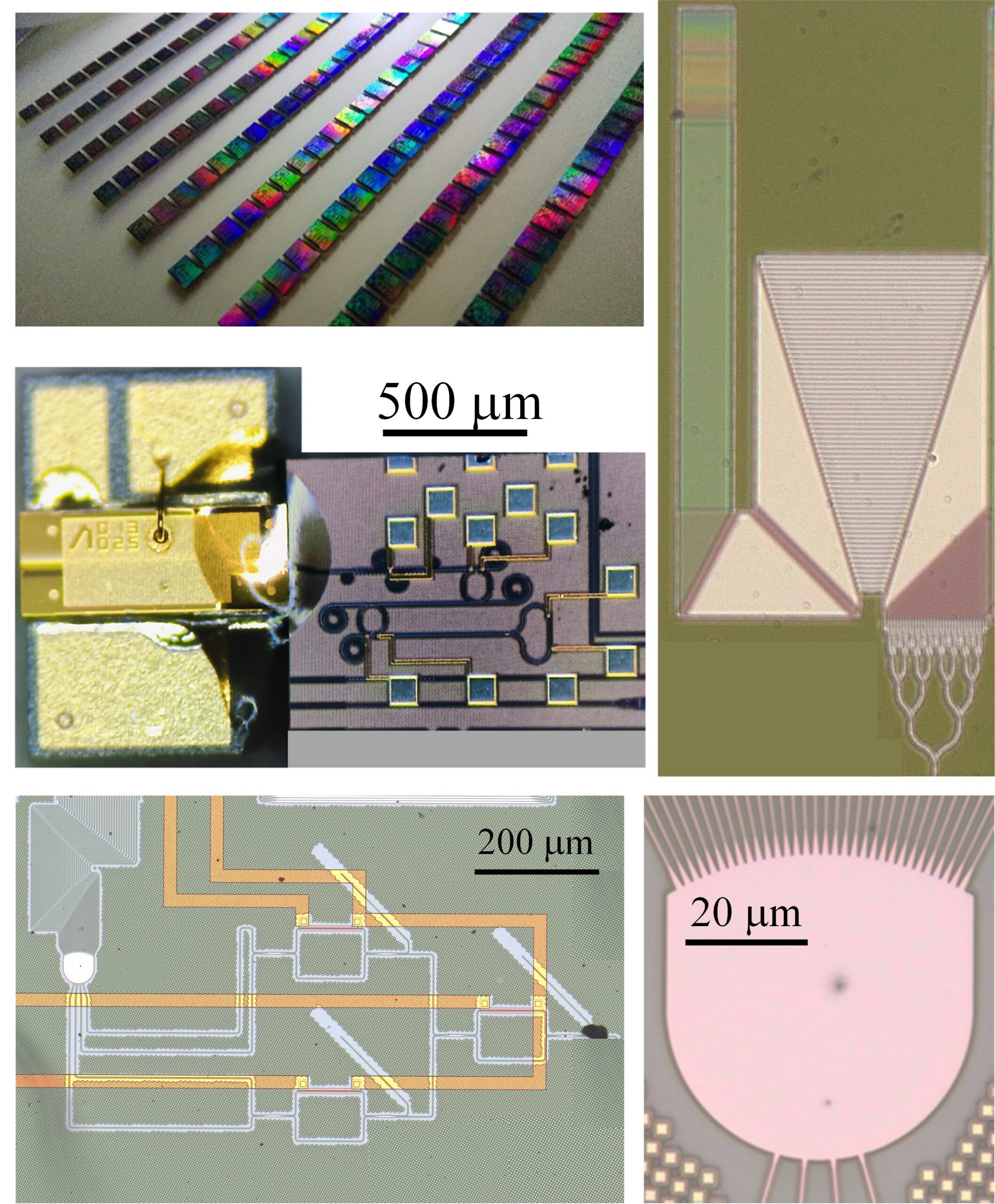
私たちの研究室では、光を使って、次世代の通信やセンサーに役立つ未来の技術を研究しています。特に、シリコンやその周辺の材料を使って、レーザや光のスイッチ、小型センサーなどを1枚のチップに集める「シリコンフォトニクス(図1)」という技術に力を入れています。これは、スマートフォンや自動運転車、次世代通信(Beyond 5G/6G)など、みなさんの生活にもこれから深く関わってくる重要な分野です。
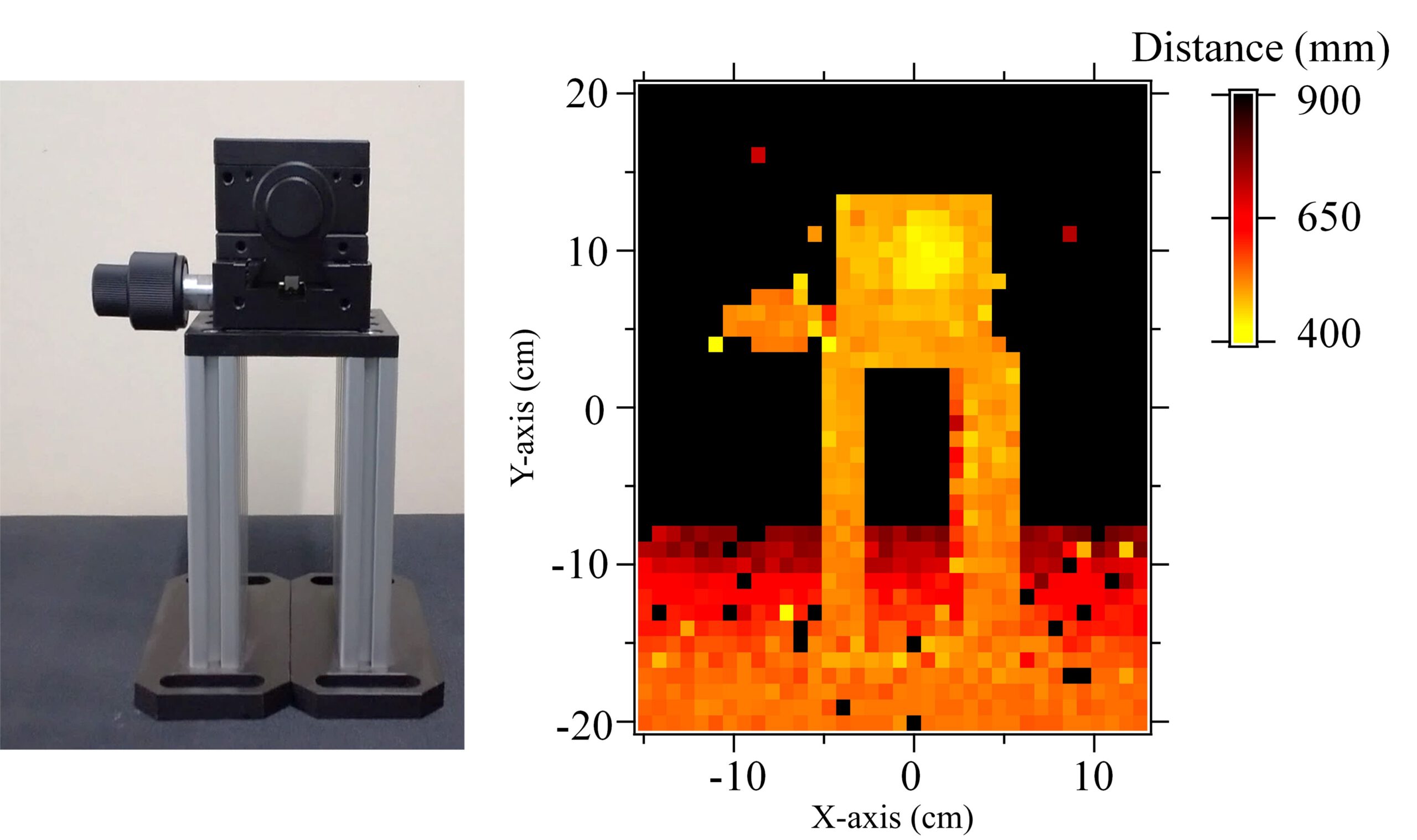
たとえば、自動運転車が周囲を認識するために使う「LiDAR(図2)」という光のレーダー技術を、もっと小さくて高性能にするための研究を行っています。私たちは、波長を細かく変えられるレーザと、光のビームの向きをコントロールできるデバイスをチップ上に一体化することで、これまでにない精度と視野を持つLiDARを実現しようとしています(図2)。将来の交通安全やロボット技術にとって、とても大きな意味を持つ研究です。
さらに、私たちの研究室では「テラヘルツ波(THz波)」という、電波と光の中間にある特殊な波を使った次世代の無線通信技術にも挑戦しています。テラヘルツ波は、今の5Gよりもはるかに多くの情報を送ることができ、映画を一瞬でダウンロードできるような通信が可能になります。私たちは、テラヘルツ波を発生させたり、受信したりするための小型チップを開発しており、それを用いた「テラヘルツ・トランシーバ」を作ることで、未来のBeyond 5G/6G通信を支えることを目指しています。
このように、私たちの研究室では「光」や「電波」を自在にあやつる技術を通じて、未来の社会をより便利で安全にすることを目指しています。研究では、コンピュータを使ったシミュレーションから、実際のチップの設計・試作・評価まで幅広く取り組むことができ、ものづくりが好きな人や、物理・数学・電子工学に興味のある人にとって、大きなやりがいのある環境です。”
MESSAGE to STUDENTS
学生へのメッセージ
光を扱う研究は、見た目以上に地道な作業の積み重ねです。試作や測定を繰り返し、思い通りに進まないことも多く、粘り強さと工夫が求められます。それでも、自分で作ったデバイスが動いたときや、美しいデータが得られたときの達成感は格別です。世界で初めてのことを自分の手で実現する。その感動は、研究ならではの体験です。ものづくりが好きな人、何かに本気で取り組んでみたい人を歓迎します。
学歴・経歴
1998年 早稲田大学理工学部電気電子情報工学科卒業
2003年 北陸先端科学技術大学院大学材料科学研究科博士後期課程修了
2003年 科学技術振興機構半導体スピントロニクスプロジェクト・博士研究員
2007年 東北大学工学研究科通信工学専攻・助教
2016年 東北大学工学研究科通信工学専攻・准教授
2018年 早稲田大学理工学術院・准教授
2022年- 早稲田大学理工学術院・教授
所属学協会
- 応用物理学会
- 電子情報通信学会
- Optica
- IEEE
Kenji YASUDA
Professor
Field of study
Photonic integrated circuit
Shaping the Future with Light, Controlled on a Tiny Chip
Research Themes
Research on photonic integrated circuits for communication and sensing applications
Keywords
Photonic Integrated Circuit (PIC), Silicon Photonics, Nonlinear Optical Effects
RESEARCH OVERVIEW
Our laboratory is conducting research to develop future technologies that use light for next-generation communication and sensing. In particular, we focus on “silicon photonics(Fig. 1.),” a cutting-edge field that integrates lasers, optical switches, and sensors on a single chip using silicon and related materials. This technology is expected to play a central role in areas closely connected to our daily lives, such as smartphones, autonomous vehicles, and next-generation communication systems like Beyond 5G and 6G.
One example of our work is on “LiDAR” (Fig. 2.), which uses light like radar to detect objects around a vehicle. This is a key technology for autonomous driving. Our research aims to create LiDAR systems that are much smaller and more precise by integrating wavelength-tunable lasers and beam-steering devices on a chip. This approach could significantly enhance the safety and performance of future transportation and robotics systems.
In addition, we are developing advanced wireless communication technologies using terahertz waves (THz waves)—special electromagnetic waves that lie between radio waves and light. Terahertz waves can carry far more data than current 5G networks, potentially enabling things like downloading full movies in an instant. In our lab, we are designing compact chips that can generate and receive terahertz waves, and we are working on creating terahertz transceivers to support the ultra-fast communication of the Beyond 5G and 6G era.
Through this research, we aim to control invisible waves of light and harness them to create a safer, more convenient society. Our work covers a broad range of activities—from computer simulations to chip design, fabrication, and experimental evaluation. This provides an exciting environment for students who are interested in making things and enjoy physics, math, or electronics.
MESSAGE to STUDENTS
Research in photonics involves steady, hands-on work. You’ll go through many rounds of fabrication and measurement, and things often don’t go as expected. It takes patience and creativity to move forward. But when a device you built finally works, or when you see beautiful, meaningful data appear, the sense of accomplishment is extraordinary. Creating something that’s never existed before with your own hands—that’s a unique experience only research can offer. If you enjoy building things or want to take on a serious challenge, we’d be happy to have you with us.
Education and Career
1998: B.E., Department of Electrical, Electronic and Computer Engineering, School of Science and Engineering, Waseda University
2003: Ph.D., Graduate School of Materials Science, Japan Advanced Institute of Science and Technology (JAIST)
2003: Postdoctoral Researcher, Semiconductor Spintronics Project, Japan Science and Technology Agency (JST)
2007: Assistant Professor, Department of Communications Engineering, Graduate School of Engineering, Tohoku University
2016: Associate Professor, Department of Communications Engineering, Graduate School of Engineering, Tohoku University
2018: Associate Professor, Faculty of Science and Engineering, Waseda University
2022–present: Professor, Faculty of Science and Engineering, Waseda University
Professional Memberships
- The Japan Society of Applied Physics (JSAP)
- The Institute of Electronics, Information and Communication Engineers (IEICE)
- Optica (formerly OSA)
- Institute of Electrical and Electronics Engineers (IEEE)