
竹内 淳 教授
Atsushi Tackeuchi
専門分野
半導体デバイス工学研究
半導体ナノ構造の一兆分の一秒を探検する
研究テーマ
半導体量子構造の超高速現象
キーワード
半導体量子構造, 超高速現象
LINKS
RESEARCH OVERVIEW
研究概要
みなさんが普段体験する最も短い時間は、どの程度の時間でしょうか。おそらく普通思い浮かべる時間は「一瞬」という時間でしょう。これは、“まばたきするほどの短い間” で、0.1 秒ほどの時間です。それでは、半導体の中で起こるもっとも速い現象はどの程度の時間で起こるのでしょう? 答は、1兆分の1秒程度の時間ということになります。「1兆分の1秒なんて想像もつかない!」というのが多くの人の感想だと思いますが、どうしてそんなに速い現象を調べるのかというと、半導体を使ったさまざまな素子(トランジスタやレーザなど)に、いっそうの高速化が要求されているからです。これらの素子が高速化されれば、より多くの情報をより迅速に処理することが可能になります。伝達される情報量の飛躍的な拡大と高速化は人類の社会に多大な貢献をすることでしょう。
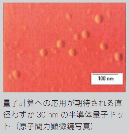
また、半導体はたんに“速い” ということにとどまらず、“非常に小さい” 人工構造物の世界です。量子ドットと呼ばれる微細な構造では、10 万分の2 ミリほどの大きさに電子の波を閉じ込めます(1nm = 10-9m)。
これを利用して演算を行うと、現在のコンピュータをはるかにしのぐ超高速の演算が期待できます(量子コンピュータと呼びます)。
半導体の世界ではまた、青色で発光するデバイスの開発が続いています。Blu-ray DVD などの日本が産んだ技術です。この青色発光半導体の研究にも取り組んでいます。
MESSAGE to STUDENTS
学生へのメッセージ
竹内研究室では、微細な半導体ナノ量子構造の中で起こる超高速の現象を調べるために、特殊なレーザから出る光パルスを使っています。光パルスの時間幅は、10 兆分の1秒という極めて短い時間です。超高速の現象を調べ、その物理を探求し、さらに応用に役立てること、それが竹内研究室のテーマです。人類の到達可能な最も速い現象を調べるということは、それだけで充分な知的冒険だと思います。若いみなさんの参加を期待しています。
学歴・経歴
2024年 高等研究所所長
2020年 研究院長
2016年 理工学術院長
2014年 先進理工学部長兼研究科長
2002年 早稲田大学理工学部・教授
1993年 マックスプランク固体研究所(独)客員研究員
1992年 博士(理学)大阪大学
1985年 大阪大学大学院基礎工学研究科博士前期課程修了.富士通研究所入社
所属学協会
- 応用物理学会
- 日本物理学会
Atsushi Tackeuchi
Professor
Field of study
Semiconductor physics
Exploring a Trillionth of a Second in Semiconductor Nanostructures
Research Themes
Ultrafast Phenomena in Semiconductor Quantum Structures
Keywords
Semiconductor Quantum Structure, Ultrafast Phenomena
RESEARCH OVERVIEW
What’s the shortest duration you usually experience? Most likely, the word “instant” comes to mind, a blink of an eye, roughly 0.1 seconds. But how fast do phenomena in semiconductors occur? The answer is about a trillionth of a second. Many might exclaim, “I can’t even imagine a trillionth of a second!” So, why investigate such incredibly fast phenomena? Because various semiconductor devices like transistors and lasers demand ever-increasing speed. The faster these devices become, the more information they can process, and the more quickly they can do it. This explosive expansion and acceleration of information transfer will significantly contribute to human society.
Semiconductors aren’t just fast; they’re also characterized by being extremely small artificial structures. In tiny structures called quantum dots, electron waves are confined to a size of about 30 nanometers (1 nm = 10⁻⁹ m). Moreover, the development of blue light-emitting devices continues in the semiconductor world. This is a technology born in Japan, applied to Blu-ray DVDs etc.. We are also engaged in research on these blue light-emitting semiconductors.
MESSAGE to STUDENTS
At Takeuchi Lab, we use light pulses from special lasers to investigate ultra-high-speed phenomena occurring within these microscopic nanostructures. These light pulses have an extremely short duration of one ten-trillionth of a second. Our lab’s theme is to investigate ultra-high-speed phenomena, explore their physics, and contribute to their application. We believe that investigating the fastest phenomena achievable by humankind is, in itself, a sufficient intellectual adventure. We look forward to the participation of young minds.
Education and Career
2024.9- Directer of Waseda Institute for Advanced Study
2020.9-2024.9 Senior Dean of Research Council
2016.9-2020.9 Senior Dean of Faculty of Science and Engineering
2014.9-2016.9 Dean of School of Advanced Science and Engineering
2002.4- Professor
1997-2002 Waseda University, Associate Professor
1996-97 Femtosecond Technology Research Association, Tsukuba, Researcher
1992-93 Max-Planck Institut FKF, Stuttgart, Germany, Visiting Researcher
1985-97 Fujitsu Laboratories Ltd., Research Scientist
1985 Osaka University, M. Eng. , 1992 Osaka University, Dr. Sci.
Professional Memberships
- The Japan Society of Applied Physics
- The Physical Society of Japan