
ページ読込中...
ページ読込中...

[English]
| 安田 賢二 [教授] |  |
|
| homepage | https://www.yasuda.phys.waseda.ac.jp | |
| 専門分野 | 生物物理学 | |
| 研究テーマ・研究活動 | ||
|
||
生物は、分子から細胞、個体に至る階層構造を持ったシステムとして機能しています。単純な原子、分子の集合化のみでは構築できない「生命」の特徴を生み出している本質はどこにあるのでしょうか。また、この「生命」の神秘はすべて物理法則のみで記述し、説明できるのでしょうか。
物理学の世界では原子、分子が規則性を持った現象論で議論をするに十分な振る舞いを見せるためにはアボガドロ数程度の要素の集合が必要ですが、生命システムの中ではわずか数個の要素を組み合わせることで巧みに高い規則性、再現性、保存性を維持することができます。これは、まさに生命システムが持つ「集団効果」であり、これを実現するための規則性、秩序をもたらす巧みな機構が生命の本質の一つなのかもしれません。
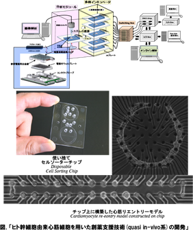 わたしたちは、この生命の各階層での要素1単位とその集団効果について、構成的な手法を用いて解明を進めています。たとえば、化学・力学エネルギー変換システムである生体分子モーターについては、その1分子の機構の解明と、これが自己組織化した筋原線維の集団的協同(振動)現象を、細胞レベルでは、心筋細胞や神経細胞1細胞の振る舞いと、これが空間配置を持って集団化したときの振る舞いの比較解析を行い、そこから「臓器モデル」ともいえる最小の細胞ネットワークチップなども構築に成功しており、創薬スクリーニングでの応用も始まりつつあります。このように、生物物理学の生物学との最大の違いは、物理法則の理解の上に立った生命現象の理解なのですが、もう一つの特徴 として、理解するために必要な技術も自分たちで創り上げています。
| Kenji Yasuda [Professor] | |
|
| homepage | https://www.yasuda.phys.waseda.ac.jp | |
| research field | Biophysics | |
| research keywords | ||
|
||
| link | ||
The cells in a group are individual entities, and differences arise even among cells with identical genetic information that have grown under the same conditions. These cells respond differently to perturbations. Why and how do these differences arise? Cells are minimum units determining their responses through genetic and epigenetic information like the history of interactions between them and fluctuations in environmental conditions affecting them. To understand the rules underlying possible differences occurring in cells, we need to develop methods of simultaneously evaluating both the genetic and epigenetic information. In other words, if we are to understand adaptation processes, community effects, and the meaning of cell network patterns, we need to analyze their epigenetic information. We thus started a project focusing on developing a system that could be used to evaluate the epigenetic information in cells by continuously observing specific examples and their interactions under controlled conditions. The importance of understanding epigenetic information is expected to become apparent in cell-based biological and medical fields like cell-based drug screening and the regeneration of organs from stem cells, fields where phenomena cannot be interpreted without taking epigenetic factors into account.
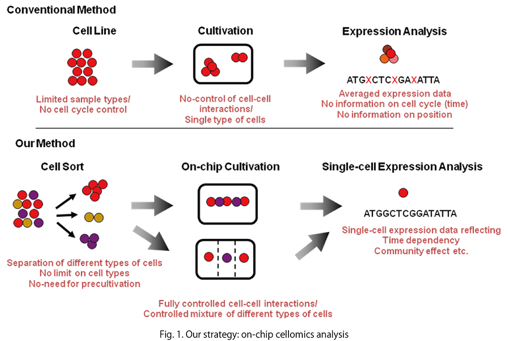
We have started a study on the “determination of genetic and epigenetic control processes in cells” using on-chip microfablication techniques and cell-based analysis. To understand the meaning of genetic information and epigenetic correlation in cells, we developed an on-chip single-cell-based microcultivation method. As we can see in Fig. 1, the strategy behind our method is constructive, involving three steps. First, we purify cells from tissue one by one in a nondestructive manner. We then cultivate and observe them under fully controlled conditions (e.g., cell population, network patterns, or nutrient conditions) using an on-chip single-cell cultivation chip or an on-chip agarose microchamber system. Finally, we do single-cell-based expression analysis through photothermal denaturation and single-molecule level analysis. In this way, we can control the spatial distribution and interactions of cells.
The first aim of our single-cell-based study was to develop methods and systems that enable the mechanism responsible for controlling (regulating) cells epigenetically to be analyzed. It is based on the idea that, although genetic information creates a network of biochemical reactions, its history as a parallel-processing recurrent network was ultimately determined by the environmental conditions of cells, which we call epigenetic information. As previously discussed, if we are to understand the events in living systems at the cellular level, we need to bear in mind that epigenetic information complements the genetic information.
The advantage of this approach is that it removes the complexity in underlying physicochemical reactions that are not always completely understood and for which most of the necessary variables cannot be measured. Moreover, this approach shifts the view of cell regulatory processes from a basic chemical ground to a paradigm of the cell as an information-processing unit working as an intelligent machine capable of adaptating to changing environmental and internal conditions. This is an alternative representation of the cell and can bring new insights into cellular processes. Thus, models derived from such a viewpoint can directly help in more traditional biochemical and molecular biological analyses that assist in our understanding of control in cells.
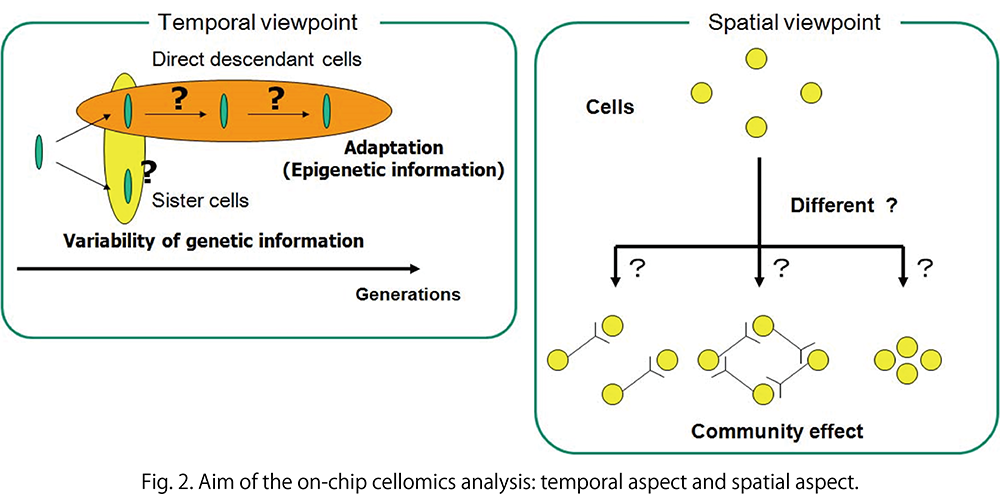
The main purpose of our study is to develop on-chip single-cell-based cultivation and analysis systems to monitor dynamic processes in the cell. We have used these systems to extend ideas from the genetic to the genetic-epigenetic network in investigating topics like variations in cells with the same genetic information, inheritance of non-genetic information between adjacent generations of cells, cellular adaptation processes caused by environmental change, the community effect of cells, and network pattern formation in cell groups (Fig. 2). After sufficient experimental observations, we can understand the role of epigenetic information in modeling more complex signaling cascades. This field has almost been entirely monopolized by physico-chemical models, which provide a good standard for comparison, evaluation, and development with our approach. The ultimate aim of our study is to provide a comprehensive understanding of living systems as products of both genetic and epigenetic information. It would permit us to describe the phenomena occurring in cell systems sufficiently well to be able to interpret and control them.
[English]
| 上田 太郎 [教授] |  |
|
| homepage | https://www.qp.phys.waseda.ac.jp | |
| 専門分野 | 生物物理学・生化学 | |
| 研究テーマ・研究活動 | ||
|
||
細胞の動きは見ていて飽きることがありません。アメーバ運動にしろ、筋肉の収縮にしろ、精子の遊泳運動にしろ、細胞の運動は、いずれもタンパク質分子モーター系とよばれる一群のたんばく質の働きに依存しています。タンパク質分子モーター系は、ATPとよばれる化学物質の分解により駆動されるので、化学エネルギーを力学エネルギーに変換するナノサイズのエネルギー変換素子と見ることができます。そのエネルギー変換機構については長い研究の歴史があり、教科書にはわかったような説明が出ています。しかし現在主流となっているそうした仮説では説明のできない現象も多々あり、大きな秘密がまだ残されていることは間違いありません。では主流派の考え方の何が問題なのかというと、激しい熱運動に晒され決定論的な動作が不可能なナノ素子の動作原理を、決定論的なメカニズムで動くマクロな機械の延長で理解しようとしているところだと思われます。われわれは、ナノサイズの分子機械の動作原理には、マクロなサイズの機械とは異なる、熱ゆらぎに基づいた動作原理があるはずだという前提に立ち、分子生物学と生物物理学の合わせ技でこの謎に迫っていこうとしています。
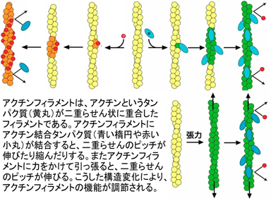
一方、細胞が適切に運動するためには、細胞各部が協調的に伸びたり縮んだりする必要がありますが、タンパク質分子モーターの活性が細胞内の場所によって異なる制御受ける仕組みはよくわかっていません。われわれは、タンパク質分子モーター系の重要な構成要素であるアクチンフィラメントが、周囲の力学環境などを感知して構造を変化させるインテリジェントな分子機械であることを見出しています。そこで、アクチンフィラメントの力学感受性が、細胞運動の統御に重要な働きをしているという仮説をたて、その検証にも挑んでいます。
生物現象は一見きわめて多様ですが、その背後に共通する基本原理を分子レベルで解明しようという姿勢が生物物理学の重要な柱になると考えています。
| Taro Uyeda [Professor] | |
|
| homepage | https://www.qp.phys.waseda.ac.jp | |
| research field | Biophysics, Biochemistry | |
| research keywords | ||
|
||
| link | ||
“Movement” is intrinsic to life. It is fascinating to observe aspects of movements such as moving cells and molecular motors under a microscope. Our goal is to understand the mechanisms of cell motility through research at cellular and molecular level. We are particularly interested in cellular slime molds as a model organism with unique characteristics of eukaryotic cell movement, and in actin filaments, one of the major components of the cytoskeletal system.
Actin is a highly conserved protein and one of the most abundant in eukaryotic cells. It is becoming clear that actin has a highly polymorphic structure and it exhibits cooperative behavior. Currently, we are mainly focused on research involving structural polymorphism and functional differentiation of actin filaments.
[English]
| 長谷川 剛 [教授] |  |
|
| homepage | https://thasega.w.waseda.jp/ | |
| 専門分野 | 物性物理学 | |
| 研究テーマ・研究活動 | ||
| 1985年 東京工業大学理学部物理学科卒業 1987年 東京工業大学大学院修士課程修了 1987-1999年 日立製作所中央研究所 1996年 博士(理学)東京工業大学 1999-2002年 理化学研究所 2002-2015年 物質・材料研究機構 2007年 文部科学大臣表彰科学技術賞(研究部門) 2015年 早稲田大学理工学術院 教授 |
||
原子の並び方ひとつで、同じ炭素原子でも、ダイヤモンドにも黒鉛にもなる。私たちが研究しているのは、そんな不思議な世界です。物質の多くは整然と並んだ原子によって構成されていますが、その表面では、物質内部とは異なる原子配列が観察されることがあります。例えば、一見平らな金の表面も原子スケールではノコギリ状であったり、シリコンの表面では原子が大きな格子模様を作っていたりします。百聞は一見に如かず。見ることができれば、沢山のことが明らかになります。新しい構造解析手法を発明した物理学者の多くがノーベル賞に輝いてきた所以です。
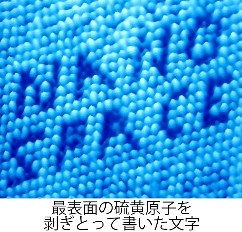
最近では、原子を観るだけでなく、個々の原子を操ることも可能になっています。例えば私たちは、二硫化モリブデンの最表面にある硫黄原子を一つずつ剥ぎ取って「原子文字」を書きました。この実験では、原子レベルで尖った針で表面をなぞって観察する「走査型トンネル顕微鏡」を用いました。原子1個を記憶単位とするメモリの開発が夢です。
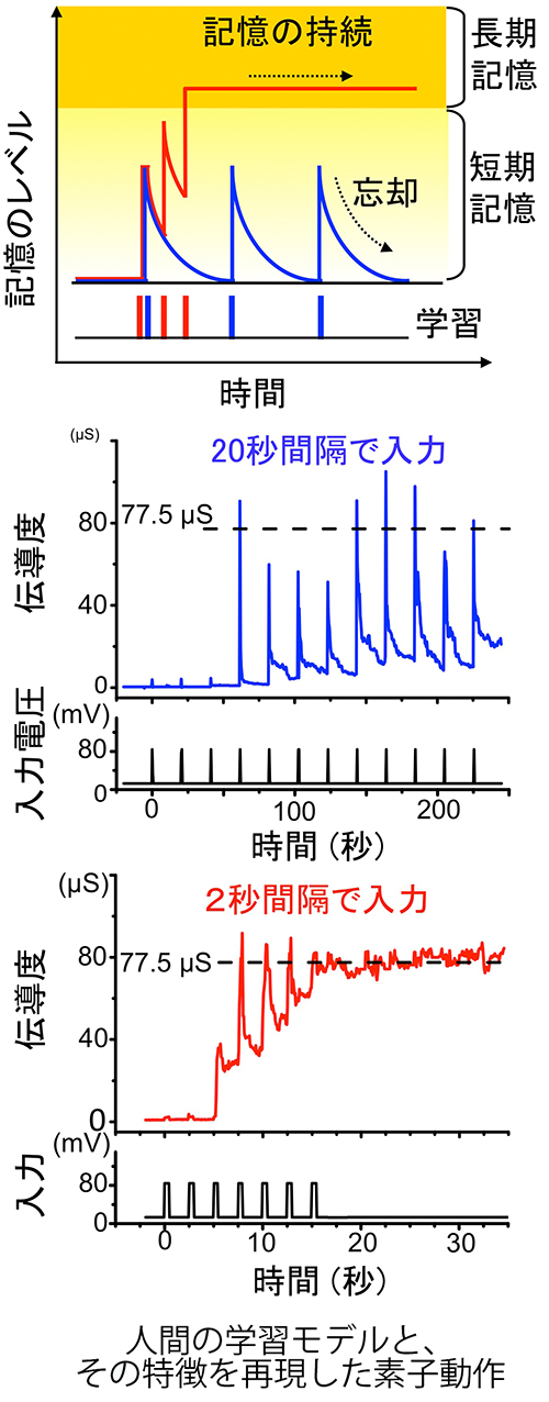
さらに、固体中を行きつ戻りつしながら原子が移動する現象を利用すると、頻繁に電圧を加えるとスイッチオンするが、時間間隔を空けて電圧を加えるといつになってもオンにならない素子も作れます。「電圧」を「学習」に置き換えると、まるで人間が何かを記憶するときと同じ様なことが起きています。
20世紀は、半導体トランジスタを始めとして、「電子」が世界の牽引役でした。一方、21世紀は、燃料電池を始めとして、「原子(イオン)」にも注目が集まっています。原子は、電子の様にトンネル効果によってどこかに行ってしまうことがありません。原子は電子よりもはるかに大きく、重たいですが、それ故に、新しい機能を実現できる可能性があります。私たちは、金属原子の輸送を制御した新しいトランジスタを世界で初めて開発しました。このトランジスタは電源を切ってもオン/オフ状態が保たれるので、起動時間ゼロのパソコンの開発に繋がると期待しています。
見方を変えれば、デメリットもメリットになります。基本物理現象の理解に基づいた新しい概念の創造を私たちと一緒にしませんか?
| Tsuyoshi Hasegawa [Professor] | |
|
| homepage | https://thasega.w.waseda.jp/ | |
| research field | Nano-science, Nano-electronics, Surface physics | |
| research keywords | ||
| Atomic switch Solid-state ionics Scanning probe microscopy Electrochemical reaction |
||
| link | ||
The same carbon atoms can be diamond or graphite depending on how they are arranged in space; the area of research that we pursue is in such a world of wonder. My research began with the graduation research to study the arrangement of atoms on material surfaces with the use of a high-resolution electron microscope. While most materials are composed of atoms in a perfect array, there are cases where atomic arrangements are observed on the surface that are different from those inside the material.
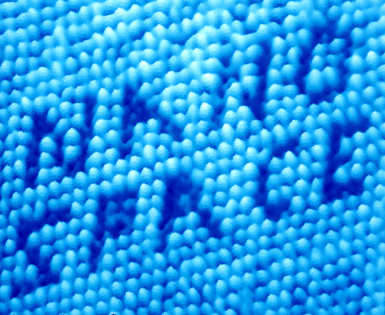
‘Atom manipulation’, which is now considered to be relatively easy to do, was a challenging research subject those days. Fig. 1 shows letters written by removing sulfur atoms from the surface of molybdenum disulfide. I worked on such tasks while I was with the Hitachi Central Research Laboratory. Hitachi values fundamental research, and I am grateful to the company for its extreme generosity.
Now my major research subjects cover clarification of phenomena on the atomic and molecular scale, and applications to devices, including the development of a new nanodevice ‘Atomic Switch’ using the transfer of atoms. I have been continuously engaged in research of ‘Observation of Atoms’, ’Manipulation of Atoms’ and ‘Utilization of Atoms’. Part of the resulting research results are in the process of being utilized for product commercialization for enterprises. All the research results were obtained with the use of uniquely developed equipment, which is required in order to pursue cutting-edge research. The conduct of research refers to reducing the number of black boxes (unknowns) one by one. So far as equipment goes, it is desirable that you should know it well enough to repair yourself, as well as understanding its principles.
We welcome students and young scientists who want to enter the nano-world.
[English]
| 溝川 貴司 [教授] |  |
|
| homepage | ||
| 専門分野 | 固体物理学・放射光分光 | |
| 研究テーマ・研究活動 | ||
| ○強相関電子系の電子状態 ○光電子分光・逆光電子分光 ○X線分光・散乱 ●日本物理学会 |
||
真空中で固体に真空紫外線やX線を照射すると表面から光電子が放出されます。この光電子の運動エネルギーと運動量を計測することにより、固体表面や固体中で電子が占有している状態を調べることができます(光電子分光)。逆に、電子線を固体表面に照射して放出される光子のエネルギーを測定することにより、電子に占有されていない状態の情報が得られます(逆光電子分光)。当研究室では、これらの電子分光に加えて、高輝度で波長可変な放射光を利用するX線分光・散乱を実験手段として、固体表面や固体中において電子の織り成す多彩な現象を、電子相関という切り口で研究しています。
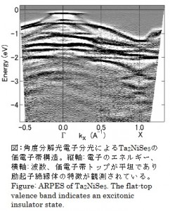 主な研究対象は、磁性や超伝導、金属絶縁体転移などの面白い物性を示す遷移金属化合物(d電子系)と希土類化合物(f電子系)です。dあるいはf電子系の電荷・スピン・軌道という自由度が格子振動と複雑に結合して、その多様な磁気的・電気的性質の発現を担っています。電子分光やX線分光による電子状態の計測結果に基づいて、物性のメカニズムを考察することができます。例えば、図のように角度分解光電子分光でバンド構造を観測し、電子間相互作用と電子格子相互作用を取り入れたモデル計算と比較することによって、電子相関や格子振動の効果を評価することができます。d電子系やf電子系は基礎物性の研究対象としての面白みだけでなく、光合成の活性中心のマンガンクラスターやリチウムイオン電池の正極のコバルト酸化物など、触媒やエネルギー変換材料としても重要です。電子分光・X線分光を駆使して表面・界面の複雑な電子状態の役割を解明することによって、従来材料の性能改善や新しい材料の開発に貢献することを目指しています。
When a solid surface is irradiated by ultraviolet or x-ray light under vacuum, photoelectrons are emitted from the surface. By measuring the energy and momentum of the photoelectrons, we can study occupied states of the solid (photoemission spectroscopy). On the other hand, we can study unoccupied states of the solid by detecting ultraviolet or x-ray light emitted from the surface under electron beam irradiation (inverse-photoemission spectroscopy). Our research interests primarily focus on electron correlation effect in various electronic states of solids that can be observed by means of the photoemission and inverse-photoemission spectroscopy as well as x-ray spectroscopy/scattering with synchrotron radiation.
In particular, we are interested in transition-metal compounds (d-electron systems) and rare-earth compounds (f-electron systems) that show rich physical properties such as magnetism, superconductivity, and metal-insulator transition. The rich phenomena are derived from the spin, charge, and orbital degrees of freedom of the d– or f-electrons that are coupled with lattice in a complicated manner. We can study their mechanisms on the basis of the electronic structural information from the electron and x-ray spectroscopy experiments. For example, band dispersion can be probed by angle-resolved photoemission spectroscopy as shown in the Figure and can be analyzed by model calculations including electron-electron and electron-lattice interactions.
In addition to the interests in the fundamental electronic structures, useful catalysts and energy materials can be developed using d– and f-electron systems such as Mn clusters for photosynthesis and LixCoO2 cathode for Li-ion battery. By proving the complicated surface or interface electronic states with electron or x-ray spectroscopy, we aim to contribute to improvement or development of future energy materials.
[English]
| 原山卓久 [教授] |  |
|
| homepage | ||
| 専門分野 | 非線形物理学 | |
| 研究テーマ・研究活動 | ||
|
1988年 早稲田大学理工学部物理学科卒業 |
||
カオスなどの非線形物理学では基礎的・一般的な数理的理論を確立することが重要です。しかし、そこにとどまらず、非線形物理学を現実世界に適用し、理論モデルが現実の複雑な世界をどの程度説明できるか、実験で測定できるものは何か、といったことを明らかにし、そこから理論研究の更なる課題と方向性を抽出することも大切です。そこで、本研究室では、非線形物理学をベースに数理的・理論的側面とそれとは真逆の応用的側面とから同時に見る視点により、様々な問題に現れるランダムネスと複雑性の起源と機能について分野横断的な研究を展開しています。
数理的な研究としては、古典力学系のカオス・量子カオス・波動カオスに関する基礎的な非線形物理学の理論研究を行っています。古典力学系のカオスの研究では、予測可能な運動と予測不可能な運動の混在する保存写像系の複雑な相空間構造を詳しく調べるという基礎研究や、運動法則が決定論的であってもカオスによってランダムウォークのような振る舞いが観測される決定論的拡散等、カオスを基礎にした新しい統計物理学の構築を行っています。このカオスとよばれる現象は軌道の不安定性を基にした概念であるため、軌道の存在しない量子力学の世界では現れません。しかし、量子現象はエネルギーが非常に大きくなると古典力学の記述に近付くはずであるという対応原理からは、古典力学のカオスの性質も量子現象に影響を及ぼすと考えられます。このような量子現象におけるカオスの顕在化を研究する学問分野が量子カオスです。また、特に量子力学的粒子の波動性に注目し、エネルギーが大きい極限、即ち、短波長極限における波動現象に対するカオスの効果として量子カオスを拡張した概念が波動カオスです。
このような理論研究を進める一方で、これらの理論的成果を非線形光学や固体物理、さらには新規デバイスに応用する研究も行っています。たとえば波動カオスに見られる複雑な共鳴波動関数がレーザーの発振状態として実現可能であることを理論的に解明し、実際に半導体レーザーなどの実験を提案し、実験研究者と協力して出射光の特性を観測しています。この実験結果から2次元的な形状の微小光共振器のレーザー発振パターンが光線カオスに由来することが明らかになります。これは、光線と波動の対応問題であり、開放型の量子エルゴード問題という深い基礎的問題の解明の必要性に繋がっています。このように、非線形物理学を現実世界に適用することで基礎的・理論的問題を浮かび上がらせることも非常に重要であると考えています。
ところで、レーザーは1次元の場合にも、出射光が反射して再びレーザーに入射する戻り光によって不安定化し、カオスを生じます。このレーザーカオスが非常に複雑な高次元カオスとなることを理論的に研究しています。戻り光レーザーカオスは、その変動が大変高速であることも特徴の一つです。この高速な不規則変化を用いると、毎秒ギガビット以上の超高速でランダムなビット列を生成することが可能になります。このように物理的に超高速で生成される乱数は、暗号など通信セキュリティにおいて重要な役割を果たします。そこで本研究室ではこのようなレーザーカオスを用いた超高速物理乱数生成をモノリシックな半導体光集積回路により実現する方法についても研究しています。そして実験研究者と協力して物理乱数生成実験を行っています。この実験から、レーザーカオスにおける量子ノイズのエントロピーソースとしての役割、小型化と高速性の関係等の理論的課題が明らかとなります。ここでもやはり応用に踏み込むことによって逆に基礎的・理論的問題を浮き彫りにしていることが、本研究室の研究スタイルの大きな特徴です。
| Takahisa Harayama [Professor] | |
|
| homepage | ||
| research field | TBD | |
| research keywords | ||
| TBD TBD |
||
| link | ||
English summary in preparation…
[English]
| 青木隆朗 [教授] |  |
|
| homepage | https://www.qo.phys.waseda.ac.jp | |
| 専門分野 | 量子光学研究 | |
| 研究テーマ・研究活動 | ||
| 2001 年 東京大学大学院工学系研究科物理工学専攻 博士課程修了、博士(工学) 2001 年 東京大学大学院工学系研究科 助手 2007 年 科学技術振興機構「さきがけ」専任研究員 (カリフォルニア工科大学滞在) 2008 年 京都大学大学院理学研究科 特定准教授 2011 年 早稲田大学理工学術院先進理工学部応用物理学科 准教授 2014 年 早稲田大学理工学術院先進理工学部応用物理学科 教授 |
||
青木研は、量子光学を中心にナノフォトニクスから量子情報まで、光科学の最先端の実験を行う研究室です。量子力学では、光(電磁場)も量子化して考える必要があり、古典光学では説明のつかない様々な不思議な性質を持っていることがわかります。このような光の量子性、および光と物質の量子力学的な相互作用について研究するのが量子光学です。本研究室では、光の量子性を実験室で実際に観測し、また光と物質の量子状態を自在に制御する技術の開発を目指します。そのためには、マイクロ~ナノスケールの光共振器や光導波路といった微小光デバイスが強力な武器となります。本研究室では、オリジナルな技術で新しい微小光デバイスを作製し、ナノフォトニクスデバイスとしての応用を探ると同時に、そのようなデバイスを量子光学の実験に適用します。
 また、光と物質の量子力学的な相互作用を通して、光を使って物質の量子状態を制御することが可能です。例えば、室温では秒速数百メートルで飛び回っている気体原子の運動を、レーザーを使って一気にマイクロケルビン(速度にして秒速数センチメートル)以下にまで冷却し、さらに捕獲することができます。このようにして極低温にまで冷却された原子は、それ自身の振る舞いに量子性が強く発現するばかりか、原子が光子を放出する過程を制御することで、自然には存在しない量子状態の光の発生に利用することができます。従来の計算機では時間がかかって計算できない問題を一瞬で計算してしまう量子コンピュータや、原理的に絶対安全(盗聴が不可能)な量子暗号などが期待される量子情報。本研究室では、光の量子性を積極的に利用し、量子情報への応用を図ります。
| Takao Aoki [Professor] | |
|
| homepage | https://www.qo.phys.waseda.ac.jp | |
| research field | Quantum Optics, Quantum Information Science, and Nano-Photonics | |
| research keywords | ||
| Quantum Optics Quantum Information Science Quantum Electronics Nonlinear Optics Nano-Photonics |
||
| link | ||
| Research Profiles (at Faculty of Science and Engineering) Research Profiles (Elsevier SciVal Experts) |
||
A cavity quantum electrodynamics (QED) system, in which an atom is coupled to the quantized electromagnetic fields (light) of an optical cavity, can be described with three characteristic parameters: g, the rate of coherent exchange of energy between the atom and cavity fields, γ, the rate of the decay of the atomic dipole, and κ, the rate of the decay of the cavity field. When the cavity has extremely high finesse and small mode volume, the condition of strong coupling, g >> γ , κ , can be achieved. In the strong coupling regime, coherent interaction of the cavity field and the atom dominates the dissipation of the system, and a single atom gives rise to a strong nonlinearity in optical responses and nonclassical statistics for light at the single-photon level, while a single photon appreciably affects the quantum state of the atom. In such a system, it is possible to generate highly quantum (nonclassical) states or to observe novel phenomena that are normally hampered by dissipation in other systems. This is applicable to quantum information science (e.g., nonclassical light sources, scalable quantum logic with photons, quantum networks connected with light), ultra-low threshold optical devices, and single atom/molecule detecting devices.
Progress in the research of cavity QED has been made with systems of single atoms coupled to Fabry-Perot cavities. In order to overcome the inherent limitation of these conventional cavities for scaling to large numbers and for coupling to single-mode optical fibers with high efficiency, the development of alternative types of cavities has been pursued.
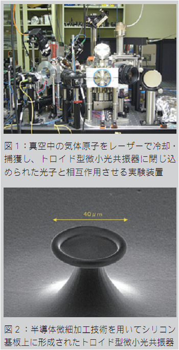
In our current research, we utilize microtoroidal resonators to build on-chip cavity QED systems. Microtoroidal resonators are fabricated by standard lithographic techniques and can be directly coupled to single-mode optical fibers with extremely high efficiency. We are currently working to build scalable multiple cavity QED systems and are seeking for applications to quantum information science with light.
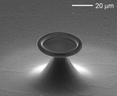
Scanning electron microscope (SEM) image of a microtoroidal resonator, which is monolithically fabricated on a silicon chip by using standard photolithography and etching techniques. The resonator’s quality factor reaches as high as 108.
[English]
| 森島 繁生 [教授] | ||
| homepage | https://morishima-lab.jp/ | |
| 専門分野 | Computer Vision 音声・音響情報処理 Computer Graphics Human Computer Interaction Accessibility Artificial Intelligence |
|
| 研究テーマ・研究活動 | ||
| 1987 年 東京大学大学院工学系研究科博士課程修了 工学博士(東京大学) 1988 年 成蹊大学工学部電気工学科・助教授 1994 年-1995 年 トロント大学・客員教授 2001 年 成蹊大学工学部電気電子工学科・教授 2004 年 早稲田大学理工学部・教授 2020 年 CG Japan Award受賞 2021 年 IBM Academic Award受賞 情報処理学会フェロー, 画像電子学会フェロー, 日本顔学会理事 |
||
物理学を応用して人々に幸福をもたらすこと、安全・安心な社会、豊かな生活、日本の伝統文化などあらゆる面で、先端技術を通して貢献するというのが、森島研の研究目標です。あくまで最終のターゲットは人間の幸福や豊かな感性・文化に向けられているというのが特徴であり、研究者の自己満足に終わらせないことが重要なスタンスです。具体的には、物理、数学を道具だてとして使いこなし、ディジタル信号処理(SP)、コンピュータビジョン(CV)、コンピュータグラフィックス(CG)、ヒューマンコンピュータインタラクション(CHI)などの最先端の研究テーマを通して、世界に技術力をアピールするだけではなく、実際に目に見えるコンテンツや具体的に役に立つシステムとして具現化し、産業界に貢献していきます。
現在、下記の5つのグループで、研究を進めています。
1)人物Modelingチーム:人物3次元モデリング 表情アニメーション バーチャルヒューマン
2)Computer Vision・AIチーム:深層学習基礎 生成AI 言語処理 DeepFake対策
3)Rendering・Simulationチーム:流体・クロスシミュレーション フォトリアル高速レンダリング
4)音楽・音響チーム:音源分離 楽器音分離 マルチモーダル認識 リップシンク 読唇
5)Human Computer Interactionチーム:視覚障碍者支援 LLM応用 英文読解支援
実用的に成功した開発技術例として、2005 年の愛・地球博で実装され、164 万人に感動を与えた“Future Cast System” があります。これは長崎のハウステンボスで常設展示化されました。現在は深層学習の時
![]() https://github.com/shunsukesaito/PIFu
https://github.com/shunsukesaito/PIFu
| Shigeo Morishima [Professor] | ||
| homepage | https://morishima-lab.jp/ | |
| research field | Physics-based Human Modeling and Image/Signal Processing Human Computer Interaction |
|
| research keywords | Computer Vision Speech/Music Signal Processing Computer Graphics Human Computer Interaction Accessibility Artificial Intelligence |
|
| link | https://researchmap.jp/futurecast | |
The research goal of the Morishima Laboratory is to contribute through advanced technology to all aspects of society, including the application of physics to bring happiness to people, a safe and secure society, a rich lifestyle, and traditional Japanese culture. Our research is characterized by the fact that our ultimate target is human happiness and enrichment of sensibilities and culture, and it is important not to end up with the self-satisfaction of researchers. Specifically, we use physics and mathematics as tools, and through cutting-edge research themes such as digital signal processing (SP), computer vision (CV), computer graphics (CG), and human-computer interaction (CHI), we not only appeal to the world with our technological capabilities, but also contribute to industry by embodying them in the form of tangible content and concretely useful systems.
One of the most successful research applications is “Future Cast System” which was presented at Expo 2005 in Mitsu-Toshiba pavilion where total 1,640,000 people enjoyed the state-of-the-art technology as a digital virtual movie actor. This system moved to Huis Ten Bosch in Nakagasiki as a permanent attraction for 12 years. Now Deep Learning era is coming, we have shifted research topic to AI-based system. One of the most impact research paper was “PIFu” at ICCV 2019 which is one of the top conferences in the Computer Vision field and it has been recognized as the pioneer research in “Neural Field”. It recorded over 1000 in the reference number only in 4 years after presentation.
[English]
| 新倉 弘倫 [教授] |  |
|
| homepage | https://niikura.w.waseda.jp | |
| 専門分野 | 超高速レーザー分光、アト秒物理 | |
| 研究テーマ・研究活動 | ||
| 2000年 総合研究大学院大学 数物科学研究科 博士後期課程修了 博士(理学) 2000年 カナダ国立研究機構(National Research Council) 研究員 2004年-2012年 科学技術振興機構 さきがけ研究員 2010年 早稲田大学先進理工学部 准教授 2012年 文部科学大臣表彰 科学技術賞(研究部門) 2013年 日本学術振興会賞 2015年 現職 |
||
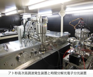
本研究室では、赤外から極端紫外領域の超高速レーザー分光・測定技術の開発と、それを用いた原子や分子の量子ダイナミックスの測定を行っています。測定の時間領域は数フェムト秒(fs, 10-15秒)からアト秒(as, 10-18秒)という極限的な領域で、この時間領域では物質(分子)の構造変化よりも早く運動する電子の刻一刻の姿を測定することが可能です。そのため本研究室では、キャリアエンベロープ位相が安定化した高強度のレーザー系(~6mJ/pulse, 1KHz, 35fs)を用いて高強度5フェムトパルスおよびパルス幅が数百アト秒以下のアト秒パルスを発生し、光電子分光法や吸収分光法と組み合わせることで、原子や分子内の電子運動やそのイオン化過程がどのように起こっているのかを時間分解で測定することや、分子の波動関数をイメージング測定する方法などを開発しています。
従来のフェムト秒科学では、分子や固体などの構造(核間距離や角度)の変化を実時間で追跡することが行われていました。しかし、反応の選択性や反応効率、また様々な物性などの発現には、電子波動関数(分子軌道)の広がりやその位相が重要な役割を果たしています。アト秒科学の方法(再衝突電子法や高次高調波分光)などを用いることで、分子構造が変化するよりも速い時間で、分子内の電子波動関数がどのように変化するのかを測定することが可能になります。特に、原子・分子内における多電子の相関過程は興味の対象になります。
 また極端紫外領~軟X線領域では、従来、コヒーレントかつパルス幅の短いレーザー光源を用いることは困難でした。これらのエネルギー領域は原子・分子の量子ダイナミックスだけではなく、マテリアルサイエンスやバイオイメージングなどにも重要な領域です。アト秒高次高調波などの様々な超高速分光法により、より速い時間領域かつ良い空間分解能で、電子波動関数(分子軌道)の変化を元にした新たな物理現象および物理化学的過程の発見を期待しています。
| Hiromichi Niikura [Professor] | |
|
| homepage | https://niikura.w.waseda.jp | |
| research field | Attoseconds and Ultra-fast Spectroscopy | |
| research keywords | ||
| Intense Laser Attosecond Physics Quantum |
||
| link | ||
| Research Profiles (at Faculty of Science and Engineering)Research Profiles (Elsevier SciVal Experts) | ||
The best time-resolution of measurements has now reached less than a few-hundred attoseconds (1attosecond = 10-18 s). In this time scale, “pure” electron motion can be explored because most molecular structural changes can eventually be frozen. Our aim is to make advancements in the methodology for ultra-fast measurements and coherent imaging technology for wavefunctions. Attosecond science develops precision measurement technologies, and has a possibility to renew quantum physics because of its excellent time-resolution and unique features for measurements. We focus on the following research subjects:
(1) Attosecond measurement
There are two approaches for attosecond science. One is to use optical pulses with photon energy in the extreme ultraviolet region, which is referred to as “high-harmonic generation.” The other is to use the electron pulses, which is referred to as the “attosecond re-colliding electron.” In both approaches one can measure nuclear and electron dynamics in attosecond time-resolution. For instance, we have measured the molecular vibrational motion of Deuterium and the electron wavepacket motion in ethane on ever-faster time scales. We further try to generate shorter pulses and to develop experimental attosecond approaches for measuring electron dynamics during complex molecular reactions.
(2) Imaging wavefunctions
What is a wavefunction Can we observe it directly A wavefunction itself is given by a complex function. According to the statement of Max Born, the square of the amplitude of the wavefunction in unit volume represents the probability to find a particle in the unit volume. On the other hand, taking the square of the amplitude of the wavefunction eliminates the information on the phase. The phase of the wavefunction is critical to understanding chemical reaction dynamics, as has been shown in Frontier Orbital theory. However, so far it has been thought that the wavefunction itself, including the phase information, cannot be observable. On 2004, we showed that attosecond “re-collision” technology made it possible to observe the wavefunction itself. Our approach, referred to as “molecular orbital tomography,” is based on the fact that tunnel ionization and electron re-collision act as a quantum optical interferometer. We will extend this approach in order to apply many molecules and measure dynamical change.
(3) Quantum control of molecules
When we shine intense, short laser pulses on a molecule, a large Stark shift is induced in the energy levels of the molecule. The amount of the Stark shift depends on both the internal and external coordinates of the molecule. Thus, applying short laser pulses to coherently created molecular wavepackets, we can align or orientate molecules, or control the atoms in a molecule. This technique is referred to as “molecular optics.” Using attosecond laser technology, we try to control electron motion in molecules according to our desires in ever faster time scales.
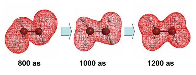
Attosecond electron wavepacket motion in ethane (C2H6). 1as = 1 attosecond = 10-18 second.
[English]
| 多辺 由佳 [教授] |  |
|
| homepage | https://tabe.w.waseda.jp/ | |
| 専門分野 | ソフトマター物理学研究 | |
| 研究テーマ・研究活動 | ||
| 1987 年 東京大学工学部物理工学科卒業 1989 年 工業技術院 電子技術総合研究所 超分子部 研究官 1996 年 博士( 工学) 東京大学 1996 年-1998 年 ハーバード大学物理学科 2005 年 早稲田大学理工学部・教授 |
||
液晶ときいて、皆さんは何を思い浮かべるでしょうか。携帯電話、パソコン、テレビなどの表示パネルを始め、薬品や化粧品などにも広く使われている他、私達の身体の中にある生体膜もまた液晶の1 種です。一般に液晶を構成する分子は棒のような形
をしていますが、このような棒状分子は液晶状態では、自由に動き回りながら常にその方向を互いにそろえようとします。この
柔らかくて強い異方的な分子間相互作用こそ液晶の特徴であり、表示パネルもこの性質を利用しているといえます。
液晶分子は、熱平衡構造で互いに向きをそろえるだけでなく、動く時も常に位相のそろった協調的な運動をしようとする性質
を持っています。私達は二次元の液晶を対象に、液晶分子の協調運動を研究してきました。厚さが数ナノメートル程度しかない
二次元液晶では、外場によってほんのわずか分子に引き起こされた変化が、三次元系と違って打ち消されることなく巨視的なダイナミクスへと発展しやすいからです。
これまで私達は、微弱な光で分子をわずかにつついた時に爆発的な分子の津波が発生したり、水を液晶膜に通過させた時に分子が集団で一斉に歳差運動をしたりするという、不思議な非平衡現象を見出してきました。柔らかく強い分子相関が主役となる非平衡ダイナミクスは、従来にない新しい液晶の可能性を与えるものであり、例えばこれを利用して、液晶ナノマシーンを実現することも夢ではないと考えています。
| Yuka Tabe [Professor] | |
|
| homepage | https://tabe.w.waseda.jp/ | |
| research field | Non-equilibrium dynamics in 2D liquid crystals | |
| research keywords | ||
| Liquid crystals Non-equilibrium dynamics in softly condensed matter Cross-coupling of molecular motion and orientation |
||
| link | ||
| Research Profiles (at Faculty of Science and Engineering)Research Profiles (Elsevier SciVal Experts) | ||
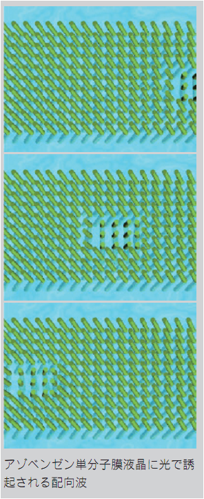
Two-dimensional liquid crystals (LCs) exhibit unique structures that cannot be found in bulk LCs. LC films of several tens of nanometer in thickness are significantly influenced by the effects of surfaces and interfaces, which, coupled with large molecular fluctuations and fluidity (flexibility), give rise to various spontaneous patterns. Due to our interest in their dynamic properties, we have investigated spatio-temporal molecular movement in LC films induced by weak photo-excitation and transmembrane gas transfer. When an LC monolayer of azobenzene derivatives is formed on a water surface and illuminated by linearly polarized green light, molecular photo-isomerization on the order of a few percent develops into a collective pendulum motion involving the molecules, observed as macroscopic orientational waves. The direction of propagation and the speed of the waves can be determined by the polarization direction and the intensity of the excitation light, respectively. The phenomenon highlights the complex nature of liquid crystallinity. How the random molecular motions couple coherently, resulting in macroscopic wave generation and propagation, is currently being examined. Another unique trait observed in 2D LCs is collective molecular precession driven by transmembrane gas transfer. In chiral LC films, molecules may be regarded as having propellers made of chiral groups, enabling them to rotate in one direction under gas flow across the film like windmills or watermills. Liquid crystalline molecular interactions gradually synchronize the unidirectional but random rotations, resulting in the collective precession clearly visible under an optical microscope. It appears that soft and strong molecular orientational interactions play an essential role in both dynamic structures, but how this motion is transformed from the vastly differing scales ranging from nm to mm and from pico-seconds to micro-seconds is not yet understood. This multi-scale energy transformation is one of the unique properties of soft matter. In addition to inherent scientific interest, an understanding of the process of transformation in the mesoscopic region will help clarify life activities and help make possible soft nano-machines.
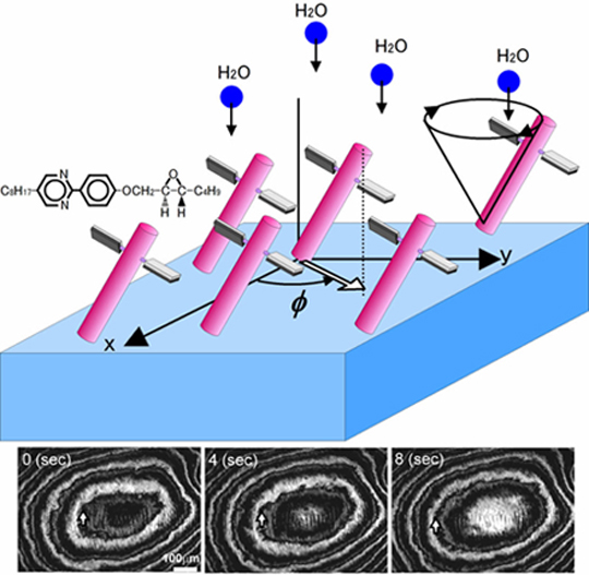
Collective precession of chiral molecules in an LC monolayer. The figure above is a schematic drawing of the system. The lower figure shows snapshots taken by a polarizing microscope. When the water vapor molecules permeate the LC monolayer, molecules with chiral propellers exhibit precession in a certain direction. The rate of precession varies linearly with differences in water vapor pressure. Inverting molecular chirality and flow direction will reverse its direction.
[English]
| 竹内 淳 [教授] |  |
|
| homepage | https://atacke.w.waseda.jp/ | |
| 専門分野 | 半導体デバイス研究 | |
| 研究テーマ・研究活動 | ||
| 1985 年 大阪大学大学院基礎工学研究科 博士前期課程修了.富士通研究所入社 1993 年 博士(理学)大阪大学 1993 年 マックスプランク固体研究所(独)客員研究員 電子情報通信学会論文賞 受賞 2002 年 早稲田大学理工学部・教授 2004 年 応用物理学会論文賞JJAP 論文賞 受賞 |
||
みなさんが普段体験する最も短い時間は、どの程度の時間でしょうか。おそらく普通思い浮かべる時間は「一瞬」という時間でしょう。これは、“まばたきするほどの短い間” で、0.1 秒ほどの時間です。それでは、半導体の中で起こるもっとも速い現象はどの程度の時間で起こるのでしょう? 答は、1兆分の1秒程度の時間ということになります。「1兆分の1秒なんて想像もつかない!」というのが多くの人の感想だと思いますが、どうしてそんなに速い現象を調べるのかというと、半導体を使ったさまざまな素子(トランジスタやレーザなど)に、いっそうの高速化が要求されているからです。これらの素子が高速化されれば、より多くの情報をより迅速に処理することが可能になります。伝達される情報量の飛躍的な拡大と高速化は人類の社会に多大な貢献をすることでしょう。
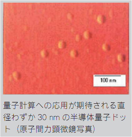
また、半導体はたんに“速い” ということにとどまらず、“非常に小さい” 人工構造物の世界です。次の写真は、量子ドットと呼ばれる微細な構造の写真(原子間力顕微鏡で撮影したもの)で、10 万分の2 ミリほどの大きさに電子の波を閉じ込めます(1nm = 10-9m)。
これを利用して演算を行うと、現在のコンピュータをはるかにしのぐ超高速で大規模な演算が期待できます(量子コンピュータと呼びます)。
半導体の世界ではまた、青色で発光するデバイスの開発が続いています。
Blu-ray DVD などの日本が産んだ新しい技術です。この青色発光半導体の研究にも取り組んでいます。
竹内研究室では、このような微細なナノ構造の中で起こる超高速の現象を調べるために、特殊なレーザから出る光パルスを使っています。光パルスの時間幅は、10 兆分の1秒という極めて短い時間です。超高速の現象を調べ、その物理を探求し、さらに応用に役立てること、それが竹内研究室のテーマです。人類の到達可能な最も速い現象を調べるということは、それだけで充分な知的冒険だと思います。若いみなさんの参加を期待しています。
| Atsushi Tackeuchi [Professor] | |
|
| homepage | https://atacke.w.waseda.jp/ | |
| research field | Manipulation of carriers and spins in semiconductor quantum confined structures | |
| research keywords | ||
| Semiconductor physics Spintronics Ultrafast phenomena |
||
| link | ||
| Research Profiles (at Faculty of Science and Engineering) | ||
Manipulation of electronic spin may provide new flexibility in device operations. Since spin in quantum dots is maintained coherently over nanosecond intervals by three-dimensional quantum confinement effects, the phenomenon may find applications in quantum memory or computing devices. Our research seeks to apply this underdeveloped flexibility for use in future quantum devices and for computing, based on our studies of ultrafast phenomena in semiconductor quantum-confined structures.
At the outset of related work, Tackeuchi realized the inadequacies of conventional time-resolved photoluminescence measurements for observations of very fast picosecond spin relaxation in semiconductors. In response, he proposed and put to use novel pump and probe measurements to observe the spin relaxation of III-V compound semiconductors. He successfully observed for the first time the picosecond spin relaxation process in GaAs quantum wells, InGaAs quantum wells, and bulk GaN. He also demonstrated many interesting aspects of luminescence and tunneling in quantum wells, quantum dots, and the GaN system.
1) “Direct Observation of Picosecond Spin Relaxation of Excitons in GaAs/AlGaAs Quantum Wells using Spin Dependent Optical Nonlinearity,” A. Tackeuchi, S. Muto, T. Inata and T. Fujii, Appl. Phys. Letters 56 (1990) pp. 2213-2215.
” First observations of picosecond spin relaxation in GaAs/AlGaAs quantum wells”
We proposed and demonstrated a novel observation method using a pump and probe technique, which enabled clear observations of picosecond spin relaxation.
2) “Dynamics of Carrier Tunneling between Vertically Aligned Double Quantum Dots,” A. Tackeuchi, T. Kuroda, K. Mase, Y. Nakata, and N. Yokoyama, Phys. Rev. B, 62 (2000) pp. 1568-1571.
“First time-resolved measurement about carrier tunneling between quantum dots”
We demonstrated that tunneling between quantum dots is one order of magnitude slower than between quantum wells.
3) “Electron Spin Relaxation in InGaAs/InP Multiple-quantum Wells,” A. Tackeuchi, O. Wada and Y. Nishikawa, Appl. Phys. Lett. 70 (1997) pp.1131-1133.
“First observation of spin relaxation in InGaAs quantum wells in which the energy bandgap corresponds to the optical communication wavelength of 1.55 micrometers”
4) “Electron Spin Flip by Antiferromagnetic Coupling between Semiconductor Quantum Dots,” A. Tackeuchi, T. Kuroda, Y. Nakata, M. Murayama, T. Kitamura and N. Yokoyama, Jpn. J. Appl. Phys., 42, Part 1, 7A (2003) pp. 4278-4281.
“First observation of formation of antiferromagnetic coupling between semiconductor quantum dots”
Antiferromagnetic coupling between quantum dots is expected to move technology further toward quantum computing.
5) “Subpicosecond exciton spin relaxation in GaN,”T. Kuroda, T. Yabushita, T. Kosuge, A. Tackeuchi, K. Taniguchi, T. Chinone, and N. Horio,Appl. Phys. Lett. 85 (2004) pp.3116-3118.
“First observation of sub-picosecond spin relaxation in semiconductors”
The wurtzite GaN was found to exhibit sub-picosecond spin relaxation.
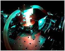
Ti:Sapphire laser (right); quantum dots (up)